Advanced Atomic Scale Characterisation
Knowledge of the atomic-scale structure, processes, and properties of advanced materials is a prerequisite for improving their properties and behavior in technological applications across a broad range of disciplines. Atomic-scale characterization makes it possible to shorten development cycles, improve lifetimes, and enable new technological innovations. Furthermore, knowledge of structural behavior and atomic-scale mechanisms provides important input for modeling and simulation.
The aim of the course is to encourage and strengthen a sustainable network of young and talented researchers between the IDEA League universities and to equip that network with improved competencies in Atomic Scale Characterisation.
Date: 12 – 16 May 2025
Where
Chalmers University of Technology; Gothenburg
Application
Application is open to PhD candidates and postdoctoral researchers of the member universities from the IDEA League Alliance.
Applications must be accompanied by a CV, motivation letter including a description of acquired experience of TEM, and a letter from the supervisor. Participation will be selected based on personal achievements.
Expenses
There are no participation or accommodation fees. Students from IDEA League member universities selected to participate in a PhD course only have to pay for their own travel (and visa) costs.
Purpose
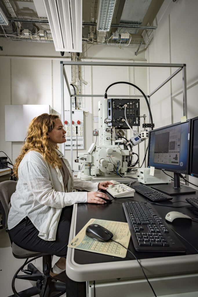
The course at Chalmers University of Technology will focus on advanced techniques for high-resolution electron microscopy, specifically for scientists currently using transmission electron microscopes in materials science studies. Laboratory sessions will showcase state-of-the-art instrumentation.
Participants should have a basic understanding of conventional electron microscope operation.
Participants
The course will be open to PhD candidates and postdoctoral researchers from the participating universities. The course specifically addresses young researchers in the following disciplines:
Chemistry, Physics, Materials Science and Engineering, and Electrical Engineering
Examples of application fields include:
Nanoscience and nanomaterials, solid state physics/chemistry, catalysis, functional materials, materials for IT, quantum materials and 2-D materials. No prior knowledge in the specific experimental techniques is needed but a basic understanding of conventional electron microscope operation is required.
Lectures
The course will feature lectures on High precision STEM
- TEM Tomography
- Image Processing
- In situ
- EDX
- EELS
- Monochromated EELS
- Differential Phase Contrast
- Electron Beam Dose Considerations
- Applications of Advanced TEM
Laboratory Sessions
The course will include laboratory sessions on:
- TEM tomography
- High precision STEM
- Monochromated EELS and Atomic Resolution EDX (JEOL 200F NEOMono)
- Specimen Preparation
The laboratory sessions will be carried out using monochromated and double-corrected JEOL-ARM200F NEOARM, the monochromated and probe-corrected Titan 80-300, the Tecnai G2 TEM and the FEI Versa 3D.

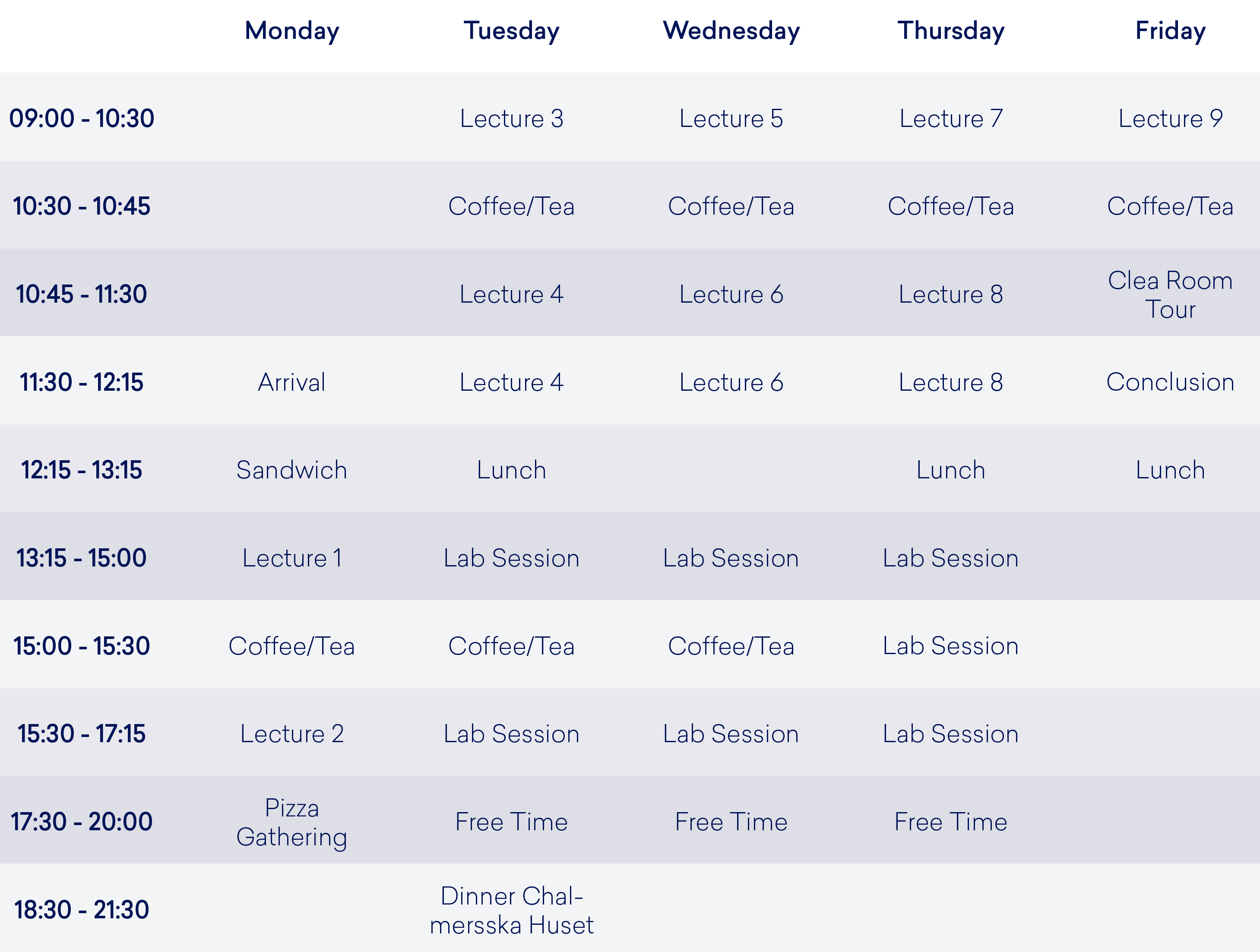
Programme

download the brochure of this PhD course here
